Working Theory Of A Full Wave Rectifier And Its Waveform

Table of Contents
Full Wave Rectifier
In a full wave rectifier, current flows through the load in the same direction during both half cycles of the AC supply's input. This is possible when two diodes alternately operate. One diode supplies current to the load during the positive half cycle of the input AC supply, and the other diode supplies current during the negative half cycle, with current always flowing in the same direction through the load. As a result, the full wave rectifier uses both half cycles of an input.
Circuit Diagram

Circuit Details
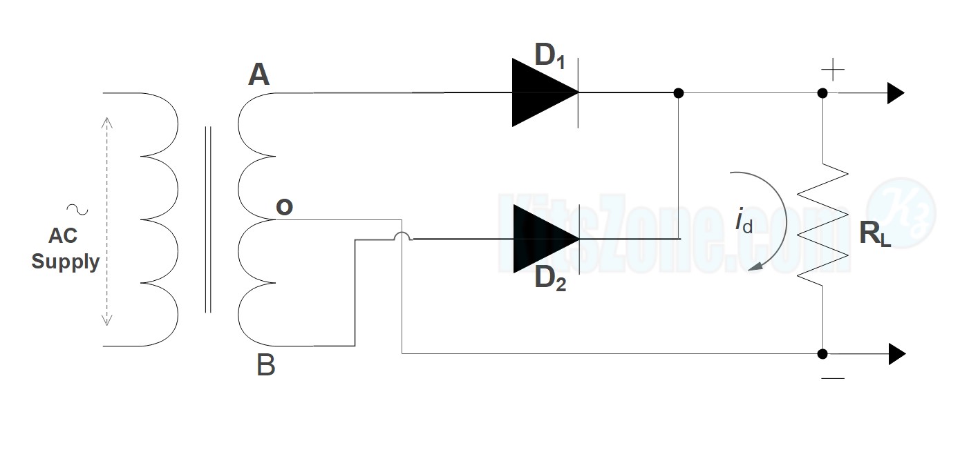
The circuit employs two diodes D1 and D2 as shown in the above figure. A centre taped secondary winding AB is utilised, with two diodes linked so that each uses one half-cycle of the input alternating current supply. In other words, diode D1 rectifies using the AC supply appearing across the upper half (OA) of the secondary winding, whereas diode D2 rectifies using the lower half winding OB.
Circuit Working
During the positive half-cycle of secondary voltage, the secondary winding's end A becomes positive and end B becomes negative. This causes D1 to be forward biased and D2 to be reverse biased. As a result, diode D1 conducts but diode D2 does not. The typical current flow is through D1, the load resistor RL, and the upper part of the secondary winding.
During the negative half-cycle of secondary voltage, the secondary winding's end B becomes positive and end A becomes negative. This causes D2 to be forward biased and D1 to be reverse biased. As a result, diode D2 is conducting but diode D1 is not. The typical current flow is through D2, the load resistor RL, and the bottom half of the secondary winding.
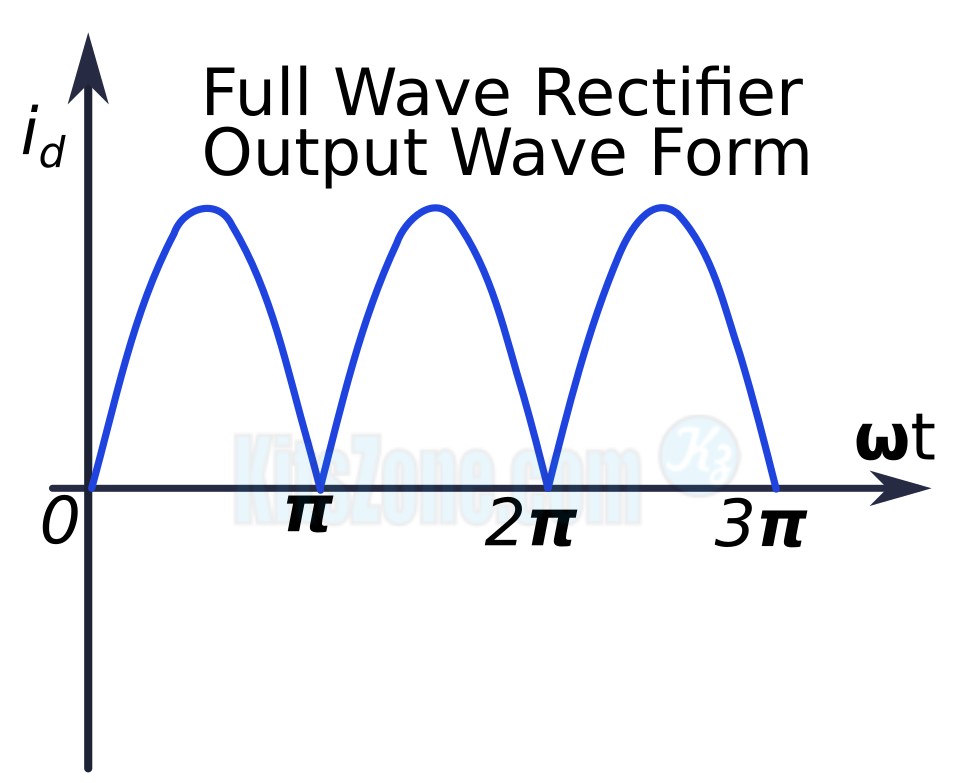
Referring to the circuit above, one can observe that the current in the load RL is in the same direction for both half cycles of the input AC supply. Consequently, DC is produced across the load RL. Additionally, the polarity of the DC output across the load must be noted.
Input And Output Waveform


Mathematical Analysis
Let diodes D1 and D2 have the same dynamic resistance Rf and be identical. At any given instant, the magnitudes of AC voltages applied to the diodes must equal
$${\rm{V}} = \,{a \over b}$$
where is the peak input voltage. Whenever one of the diodes is conducting, the total circuit resistance is Rf + RL, ignoring the secondary resistance of the transformer.
Comparing the values of both e, we get
where is the peak current.
If the resistance of the diode is negligible compared to RL,
From the output waveform of second graph, we can represent,

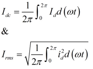
DC Value of Current (Idc)
From the output waveform, it is seen that the output current is not steady but contains fluctuations despite of being a DC current. The average value of this fluctuating DC current can be calculated as follows:

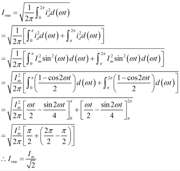
RMS Value Of Current (Irms)

Efficiency


From the value of , we can confirm that the efficiency of full wave rectifier is double to that of a half wave rectifier.
Ripple Factor (r)
where I'rms and E'rms represent the RMS value of ripple current and voltage respectively.
Instantaneous value of ripple current I' = id – Idc
Using the below equations,

we have,
Ripple Factor is given by,

Peak Inverse Voltage
It is defined as the maximum voltage applied across the diode when the diode is reverse biased. In a full wave rectifier, the peak inverse voltage across the diode D1 can be found out to be the maximum voltage across D1 when D1 des not conduct and D2 conducts. In a center tapped transformer when the point A is at the maximum negative voltage E0, the point C is at the maximum positive voltage E0 with respect to the center tap. The voltage drop across D2 is almost zero while in conduction so that the point D is at a maximum positive voltage E0. Therefore PD between A and D across D1 is 2E0, Likewise, the peak inverse voltage across D2 will also be 2E0. Therefore in a full wave rectifier, the diodes will be subjected to a reverse voltage twice larger than that of the peak input voltage. In designing a full wave rectifier with two diodes, care should be taken to see that the selected diode must withstand this reverse voltage without any break down.


Comments